
TL;DR

Get your next haul delivered free — and shop member deals
- Fast, free delivery on millions of items
- Access to Prime Big Deal Days deals on October 6–7
- Prime Video, Amazon Music and more included
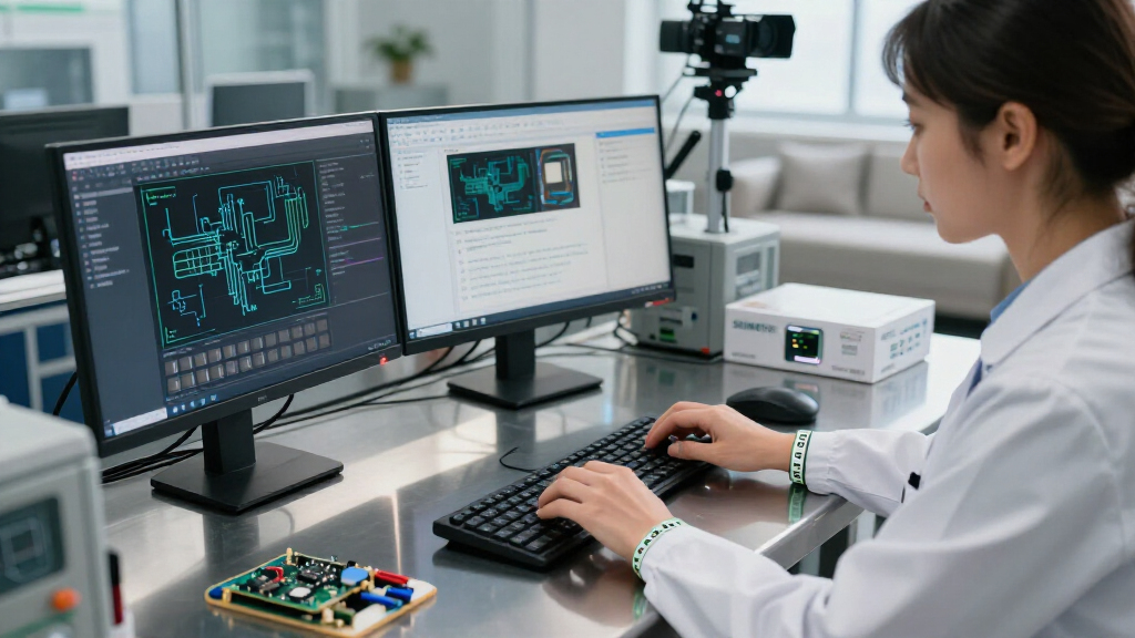
Siemens has introduced advanced self-verifying agentic AI workflows for semiconductor and PCB design. This innovation aims to enhance automation and reliability in chip manufacturing, with potential industry-wide impacts.
Siemens has announced the development of self-verifying agentic AI workflows designed specifically for semiconductor and PCB design. This innovation aims to automate complex design verification processes, potentially reducing errors and accelerating production timelines. The company states that these workflows represent a significant advancement in AI-driven automation for electronics manufacturing, addressing longstanding industry challenges.
Siemens’ new AI workflows incorporate self-verification capabilities that enable the system to automatically check and validate design outputs during the process. According to Siemens, this reduces the need for manual review and minimizes the risk of errors that can lead to costly manufacturing defects. The workflows are described as agentic, meaning they can independently make decisions and adjustments within predefined parameters, enhancing overall design efficiency. The company highlighted that these workflows are tailored for use in semiconductor fabrication and PCB layout processes, fields where precision and reliability are critical. Siemens claims that early testing indicates these AI systems can significantly shorten development cycles while improving the quality of final products. The announcement was made via a press release on PR Newswire, with Siemens emphasizing the potential for these workflows to transform electronics manufacturing by integrating AI that is both autonomous and trustworthy.Implications for Semiconductor Manufacturing Efficiency
This development matters because self-verifying AI workflows could drastically reduce the time and cost associated with semiconductor and PCB design. By automating verification and decision-making, manufacturers can accelerate production cycles and decrease human error, leading to higher yields and more reliable chips. The agentic nature of the AI suggests a move toward more autonomous manufacturing processes, which could reshape industry standards and competitiveness. Additionally, this innovation addresses the growing complexity of chip designs, which increasingly require sophisticated validation methods.
semiconductor design verification tools
As an affiliate, we earn on qualifying purchases.
As an affiliate, we earn on qualifying purchases.
Industry Challenges in Semiconductor and PCB Design
Current semiconductor and PCB design processes involve multiple manual verification stages, which are time-consuming and prone to human error. As chip complexity increases, traditional workflows struggle to keep pace, leading to delays and higher costs. AI has been gradually integrated into these processes, but fully autonomous, self-verifying systems have yet to become mainstream. Siemens’ announcement follows a broader industry push toward automation and AI-driven validation, aiming to meet the demands for faster, more reliable manufacturing cycles amid global supply chain pressures.
“Our new AI workflows are designed to independently verify and adapt during the design process, reducing errors and speeding up production timelines.”
— Siemens spokesperson
As an affiliate, we earn on qualifying purchases.
Unanswered Questions About AI Verification Capabilities
It is not yet clear how extensively these AI workflows can handle the full complexity of modern semiconductor and PCB designs or how they will perform in real-world manufacturing environments. Siemens has not disclosed detailed technical specifications or deployment timelines, and industry experts are awaiting independent validation of the system’s effectiveness and reliability under diverse conditions.
AI-driven semiconductor testing equipment
As an affiliate, we earn on qualifying purchases.
As an affiliate, we earn on qualifying purchases.
Next Steps for Adoption and Validation
Siemens plans to conduct further testing and pilot programs with select industry partners over the coming months. The company has indicated that broader commercial availability of these AI workflows could occur within the next year, contingent upon successful validation and integration. Industry observers will be watching for independent assessments and case studies demonstrating real-world performance and benefits.
self-verifying PCB layout software
As an affiliate, we earn on qualifying purchases.
As an affiliate, we earn on qualifying purchases.
Key Questions
How do Siemens’ AI workflows verify designs automatically?
They incorporate self-verification algorithms that check design outputs during the process, making adjustments as needed without human intervention, thereby reducing errors and speeding up development.
Will this technology replace human engineers in design verification?
Siemens states that the workflows are designed to augment human efforts by automating routine verification tasks, but human oversight will still be necessary for complex decision-making and validation.
When will these AI workflows be available for industry use?
Siemens has indicated that pilot programs are underway, with potential commercial release within the next 12 months, pending successful validation.
What are the main benefits of self-verifying AI in manufacturing?
Benefits include faster design cycles, reduced errors, lower costs, and increased reliability of semiconductor and PCB products.
Are there any risks associated with autonomous AI workflows?
Potential risks include over-reliance on automation, unforeseen errors in complex designs, and integration challenges, which Siemens and industry regulators will need to address.
Source: primary
Fall Picks
fall essentials
As an affiliate, we earn on qualifying purchases.